Hardware
This section provides basic info on the wESP32™ hardware. For more details, please refer to the wESP32 Product Brief.
GPIO header pinout
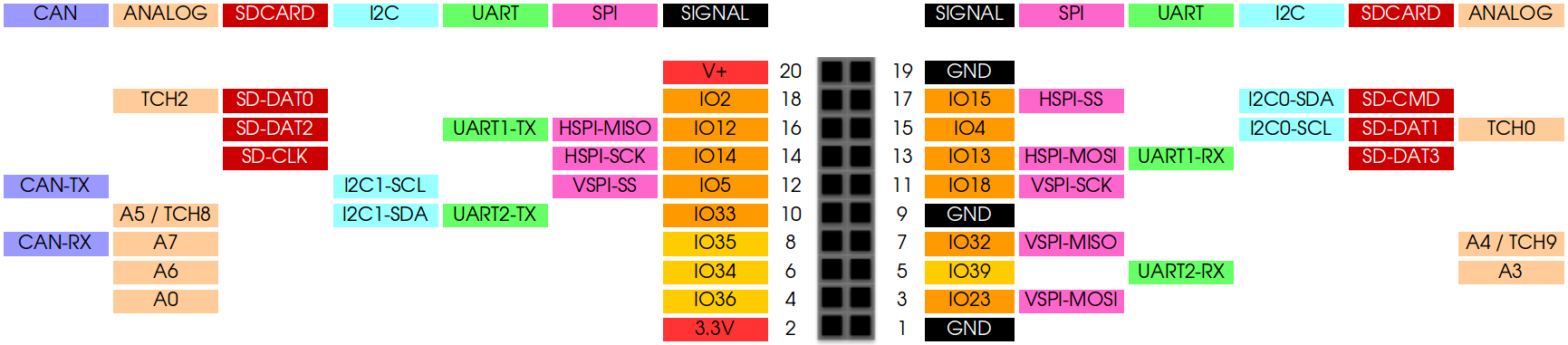
| Pin | Signal | SPI | UART | I2C | SDCARD | ANALOG | CAN |
|---|---|---|---|---|---|---|---|
| 1 | GND | ||||||
| 2 | 3.3V | ||||||
| 3 | IO23 | VSPI-MOSI | |||||
| 4 | IO36 | A0 | |||||
| 5 | IO39 | UART2-RX | A3 | ||||
| 6 | IO34 | A6 | |||||
| 7 | IO32 | VSPI-MISO | A4 / TCH9 | ||||
| 8 | IO35 | A7 | CAN-RX | ||||
| 9 | GND | ||||||
| 10 | IO33 | UART2-TX | I2C1-SDA | A5 / TCH8 | |||
| 11 | IO18 | VSPI-SCK | |||||
| 12 | IO5 | VSPI-SS | I2C1-SCL | CAN-TX | |||
| 13 | IO13 | HSPI-MOSI | UART1-RX | SD-DAT3 | |||
| 14 | IO14 | HSPI-SCK | SD-CLK | ||||
| 15 | IO4 | I2C0-SCL | SD-DAT1 | TCH0 | |||
| 16 | IO12 | HSPI-MISO | UART1-TX | SD-DAT2 | |||
| 17 | IO15 | HSPI-SS | I2C0-SDA | SD-CMD | |||
| 18 | IO2 | SD-DAT0 | TCH2 | ||||
| 19 | GND | ||||||
| 20 | V+ |
Pin 1 is by the mounting hole that is not plated.
The pins used for many peripherals can be dynamically adjusted, these are default mapping of peripherals when using the Arduino development environment (and other environments with the concept of “board files” follow this layout). Please note that other development environments such as ESP32-IDF and MicroPython provide more flexibility, and allow many of these functions to be mapped to any available pin. However, if compatibility with future add-on boards that work with Arduino is desired, it may make sense to stick to these mappings even for those development environments.
NOTE: This default pinout was changed from the original documentation at release. The original pinout had I2C0-SDA on IO2, but since this pin needs to be held low to correctly enter the serial bootloader for programming, this was a bad choice for an I2C pin since I2C requires a pull-up. Also, UART1-RX used to be on IO12, which could cause issues with selecting the wrong flash voltage if an idle UART bus was connected at boot that pulled this pin high. So UART1-RX and UART1-TX are now swapped. Please ensure that your application does not pull either IO2 or IO12 high during boot and use the current default pin assignments instead of the old ones.
Programming port pinout
| Pin | Name |
|---|---|
| 1 | IO0 (DTR of programmer) |
| 2 | EN (RTS of programmer) |
| 3 | GND |
| 4 | TXD (RXD of programmer) |
| 5 | RXD (TXD of programmer) |
| 6 | V+ |
Pin 1 is toward the middle of the board, pin 6 near the edge of the board.
Heat sink mounting hole
The plated mounting hole by the Ethernet jack can be used to sink heat away from the PD controller when using high output power. Please note that this hole is electrically connected to the PSE and not locally isolated, so it should not be connected to any metal that can be touched by the user.
5V solder jumper
By default the wESP32 V+ voltage is 12 V. When this is selected, 13 W of power is available. If you bridge the "5V" solder jumper, the V+ voltage is 5 V with a reduced power of 5 W.
HG solder jumper
By bridging the "HG" solder jumper, the plated mounting hole can be used to connect the isolated circuit ground to local ground. This should not be electrically connected to the plated mounting hole by the Ethernet jack as this would negate the isolation.
Revision changes
The board revision can be found next to the Ethernet jack. From revision 7 onward, a 4-layer PCB with 1 oz copper is used, while older revisions use a 2-layer PCB with 2 oz copper.
From revision 7 onward, the ESP32 module is an ESP32-WROOM-32E with 16 MB of flash, while older revisions used an ESP32-WROOM-32 module with 4 MB of flash. No software change is required, the boards with 16 MB of flash will work fine with images created for modules with 4 MB of flash, but the software has to be changed if the user wants to take advantage of the extra flash.
From revision 7 onward, the board uses an RTL8201FI Ethernet PHY chip for increased reliability versus older revisions that used a LAN8720AI Ethernet PHY. A software change is necessary to support the new PHY. In most cases, the only thing that changes is the definition of the PHY declared in the code.
From revison 8 onward, a Sparkfun Qwiic connector is available.
3D models
A customer kindly provided this basic 3D model for SketchUp that can be helpful for designing a case. Another customer kindly shared their wESP32 case design for SketchUp that can be used as a base for other cases.